Read this article if you want to know what’s inside the peculiar blob-like assembly called a Chip on Board.
Introduction
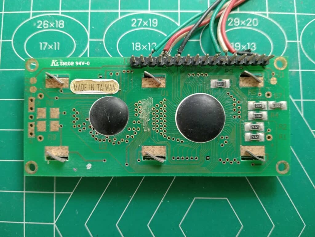
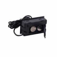
You may have found a strange-looking component that looks like a black blob connected to PCB traces when opening the assembly of some cheap electronic products. Examples of these products may include electronic toys, LCDs, calculators, and the like. These are actually complete integrated circuits embedded in the PCB itself. In this article, you’ll learn a lot about this technology which is called COB (or a Chip On Board).
What is a COB?
COB (Chip On Board) is a manufacturing process where a die (or silicon wafer slice) is placed on top of a PCB, wire bonded to the PCB pads, and encapsulated with an epoxy or plastic material. COBs were made to lower the cost or save space on an actual product.
The Advantages of Using COBs
No IC packaging is required.
Space saving. You can place more components on your board. You can also have more vertical clearance available.
Economical in volume runs since there is no IC packaging. Additionally, no formal datasheets are needed for the IC.
In automotive and industrial applications, the encapsulation makes for sturdier and thermally enhanced components.
Shorter lead lengths mean power and thermal efficiency. Also favorable for RF circuits.
What's Inside a COB and HOw is it Made?
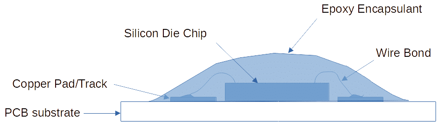
A COB is composed of a bare IC (or die), wire bonds, and epoxy encapsulation materials. The process of making a COB is explained below.
First, a PCB is fabricated along with traces and exposed pads that will connect to the silicon die wafer. In the middle of the pads is the exposed substrate of the PCB.
An adhesive material is applied on the exposed substrate of the PCB to hold the die in place.
The die is placed carefully on the PCB substrate taking into consideration that the die pads align with the PCB trace pads.
A wire bonding machine is used to connect the die pads to the PCB pads. The wire bond is usually composed of gold or silver wires.
After the wire bonding is finished its time to protect the COB assembly from the outside environment. An encapsuation material (usually expoxy) is poured into assembly and made to harden.
Other Use of COBs
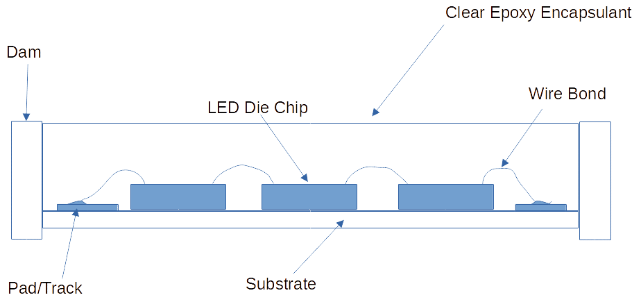
COBs come in different forms. They have varied applications and this includes the one mentioned above. Additionally, COBs are widely used in LED applications (using a clear epoxy encapsulant). The power and thermal efficiency properties of COBs are perfectly fit for LED applications.
Above is an application where multiple LED dies in series are wire-bonded together and placed as chips on board. This method makes the light generated by the group of LED dies appear more compact compared to individual SMD LEDs crammed together.
Will You have an Opportunity to Fabricate COBs?
If you’re an electronic hobbyist creating hobby projects, the chances are small that you will need to manufacture using COBs. The setup cost of COBs is high and there are most likely already discrete integrated circuits available on the market for your particular application.
However, if you’re selling by the thousands, you may consider COBs. It can save you on the cost of integrated circuit packaging as well as maximize space on your boards.